


From the Factory Floor: 4 Critical Stencil Manufacturing Tips to Save Your SMT Assembly 🛠️
 View
View
The difference between a "good" stencil and a "perfect" one often comes down to the manufacturing choices you make before hitting that order button.
To ensure your PCB assembly is fast, clean, and defect-free, here are 4 Manufacturing Key Points we recommend focusing on:
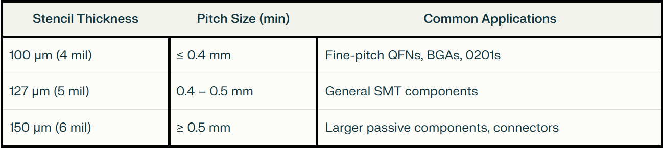
Stencil Thickness Selection
The thickness of the design determines how much solder paste is applied. Focus primarily on the smallest pitch component on the board. Solder paste may adhere to the inner walls of the aperture in a thick stencil because of a phenomenon known as surface tension. A basic rule is that there should ideally be at least five solder particles in the smallest aperture.
Stencil Material
The type of material used to make the stencil will determine how well it removes solder paste from the apertures. Even though stainless steel is typically utilized, PCB designs that use fine pitch components can employ nickel, which is around 50% more expensive than stainless steel.
The first generation of stencils were made by chemical etching, which was effective for larger apertures but became increasingly challenging to remove solder from as component sizes decreased. This resulted in the creation of laser-cut stencils, which enhanced paste release by producing a much finer, trapezoidal-shaped aperture. As component sizes shrank, the potential for electropolishing the aperture walls and, later, the method of electro-forming the stencil were developed.
Apply Nano-Coating for Improved Paste Release
Hydrophobic coatings are used in contemporary nano-coated stencils to lessen solder paste adhesion to the aperture walls. This is essentially a straightforward procedure used to apply a layer of nanomaterial on a plain stencil. What is this layer going to do? It increases solder paste release, prolongs stencil life, and lowers cleaning frequency.
Consider Step Stencils for Mixed Assemblies
This is further divided into two parts:
Step-up stencils: Thicker regions for larger components.
Step-down stencils: Thinner regions for fine-pitch components.
It is used with boards having 0201 passive components and large connectors. We have covered a full detailed article on this topic, see from here.
🔥 Custom Precision, Powered by JLCPCB
At JLCPCB, we support full customization to turn your design into reality. Our high-precision manufacturing ensures your PCB assembly is completed faster, better, and with pro-grade results.
- 🎁 Claim your $10 Stencil Coupon, and get your customized PCB Stencils here!
- 🚀 First user? Sign up to unlock your $123 Welcome Bundle.
Sign In Or Register Comment after
No comments yet. Be the first to comment!